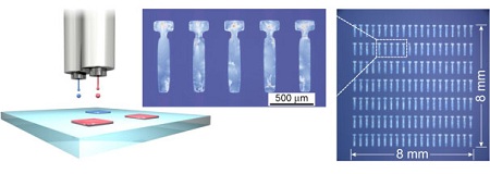
The technology allows improving performance of thin-film transistors (TFTs), indispensable building blocks for large-area electronics products such as flat displays. The performance is 100 times as high as that of TFTs fabricated by conventional printing methods.
Additionally, the films were confirmed to be single crystals using the facilities at High Energy Accelerator Research Organisation (KEK).
The printable electronics technology is expected to deliver lightweight, thin, and impact-resistant information terminal devices, such as flexible electronic devices, while at the same time saving energy and resources.
The researchers succeeded in producing single-crystal thin films of organic semiconductors with molecularly flat surfaces by the use of a novel "double-shot inkjet printing" technique. The technique uses alternating print deposition of microliquid droplets both of ink composed of a dissolved organic semiconductor and of another ink that prompts crystallisation of the organic semiconductor.
The organic TFTs based on this technology present mobility of 31.3 cm2/Vs, much higher than that of amorphous silicon TFTs that are used in the conventional liquid-crystal displays. The mobility value is also 100 times as high as that of organic TFTs produced by the conventional printing methods, and is the highest among organic TFTs reported so far.
It is expected that the technology will greatly accelerate the research and development of flexible electronic devices.
The printing technology, which is used to reproduce characters or pictures such as photographs on papers, already attracts considerable attention, since it can be used as a new manufacturing technology for electronic devices by the print production of fine electronic circuits at micrometre resolution on a sheet.
For example, replacing a vacuum film-formation process and lithography should make large-scale and high electricity-consuming vacuum facilities unnecessary in the production of large-area electronic devices such as flat displays.
Furthermore, the use of plastic sheets should lead to advances in lightweight, thin and impact-resistant characteristics for flexible electronics products.
AIST has been widely promoting the research and development of the printable electronics technology. One part of the R&D has focused on organic semiconductors which are soluble in organic solvents and can be processed at ambient pressure and temperature.
It is known for organic semiconductors that high-mobility devices are obtained by using highly-crystalline low-molecular-weight organic materials.
However, it is difficult to control the crystallisation of semiconductor materials in solution due to the convection flow and random crystallisation inside the droplets, so until now it has been considered to be extremely difficult to form a uniform semiconductor layer by conventional printing techniques.
In this study, the researchers developed the double-shot inkjet printing technique which uses alternating print deposition of microliquid droplets both of ink composed of a dissolved organic semiconductor and of another ink that prompts crystallisation of the organic semiconductor, and succeeded in producing single-crystal thin films of organic semiconductors with molecularly flat surfaces.
Moving forward the researchers plan to further optimise the printing conditions, semiconductor materials, and device structures, and improve the device performance and stability.
They also plan to manufacture high-performance active backplanes with the whole printing process, by combining the various printing techniques such as printing of metal wires and electrodes.

